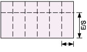
Scribed substrates
Laser Tech. will provide scribed substrates to the customers desired application
General tolerances for economic manufacture are:
| Length/Width | |
 | Tolerance between the scribed edges is substrate thickness dependent. |
| Thickness | Standard tolerance L/W |
| 0,38 mm | + 0,15 - 0,025 |
| 0,50 mm | + 0,15 - 0,025 |
| 0,635 mm | + 0,20 - 0,05 |
| 1,00 mm | + 0,30 - 0,05 |
| 1,27 mm | + 0,30 - 0,05 |
| Length/Width | |
 | Tolerance between the scribed edges is substrate thickness dependent. |
| Thickness | Standard tolerance E/S |
| 0,25 mm | + 0,10 - 0,025 |
| 0,38 mm | + 0,10 - 0,025 |
| 0,50 mm | + 0,10 - 0,025 |
| 0,635 mm | + 0,20 - 0,05 |
| 1,00 mm | + 0,30 - 0,05 |
| 1,27 mm | + 0,30 - 0,05 |
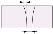
| Scribeline/Scribeline | ||
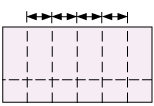 | Tolerance S/S ± 0,05 mm, typical ± 0,035 mm |
|
| Width of waste to Edge | ||
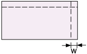 | Edge waste to be snapped off should min. be 5 times substrate thickness (min. 3 mm) | |
| Pitch/Depth | ||
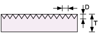 | The scribing Pitch (pulse to pulse center distance) and Depth is determined by the application and the substrate thickness. The general design rule is: |
|
| Substr. thickness | Depth | Pitch |
| 0,25 mm | 0,12 ± 0,05 | 0,14 ± 0,02 |
| 0,38 mm | 0,15 ± 0,05 | 0,14 ± 0,02 |
| 0,50 mm | 0,25 ± 0,05 | 0,16 ± 0,02 |
| 0,635 mm | 0,25 ± 0,05 | 0,16 ± 0,02 |
| 1,00 mm | 0,40 ± 0,05 | 0,17 ± 0,02 |
| 1,27 mm | 0,65 ± 0,05 | 0,17 ± 0,02 |
Advanced scribing possibilities
Laser Tech’s unique laser technology makes previous impossible scribing pattern possible
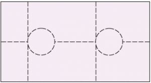 | Scribing of disc substrate possible by use of LFL. |
| Scribing of disc substrates down to 0 10 mm is an extremely cost efficient and reliable process, which only is possible by use of LFL offered by Laser Tech. | |
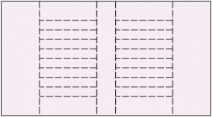 | Snapstrate with interrupt scribing pattern. |
| For more information on dimensional tolerances, please contact Laser Tech's technical sales department. | |
Laser drilling and profiling
Laser Tech will provide the combined laserdrilled, -profiled and -scribed substrates to the customers desired specification. General tolerances for optimized economic manufacture are:
| Length/Width | ||
| Tolerance between the profiled edges � 0,050 mm (± 0,002") typical ± 0,035 mm. |
|
| Holes | ||
 | Min. drilled hole size 0 0,1 tolerance | + 0,030 - 0,010 |
| Min. hole size (one shot) 0 0,075 mm (0,003") Max. drilled hole size limited by substrate size, tolerance ± 0,05 mm (± 0,002") Hole size is measured on the laser beam exit side. |
||
| Hole Center/Hole Center | |
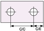 | Tolerance profiled Edge to hole Center ± 0,050 mm (0,002") Hole center to hole center ± 0,05 (0,002") |
| Hole Taper | |
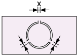
 | Taper angle "" 3° min. 0 laser beam exit |
General design rules for optimized economic manufacture are:
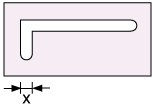
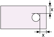 | X � Substrate thickness Distance between hole edge and substrate edge should min. be � the substrate thickness. |
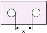 | X � Substrate thickness Hole edge to hole edge distance should min. � the substrate thickness. |
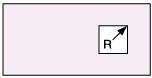 | R � 0,1 mm Avoid designs with internal sharp corners, try to design with a corner radius of min. 0,5 × the substrate thickness to minimize the risk of micro cracking. |
 | X � 0,04 mm Any profiled shape can be cut according to the customers requirement. Min. cut width ~ to 0,04 mm |
 | X � 0,1 mm Profiled disc with holding tags, of minimum 0,1 mm width. (substrate thickness dependent) |
With request of improved tolerances and designs in conflict with the general design rules please contact Laser Tech.’s technical sales department for possible available improvements.
PrimEdge™ and Super PrimEdge™
The rational answer to improved thickfilm yield and the most economical solution to quality edge finish.
PrimEdge™
Advantages and benefits:
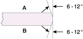
- Surface and bottom edge equally treated, for identical use of A and B
- Dimensional tolerances better than on standard scribed
- No edge chipping by substrate handling.
- Reduced laser edge stresses (edge microcraks).
- No torn printing screens due to rough and sharp
- Reduced location pin wear (better printing repeatability).
All benefits are leading to a higher production yield, to a cost only slightly higher than for a standard scribed substrate.
Super PrimEdge™
High tolerances:
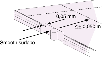
± 0,050 mm from alignment slots to any hole or scribeline on the substrate.
Alignment slots standard 4×5 mm (or more) to be placed according to customer requirements.
The ultimate answer to quality edge finish and superior printing repeatability for “state of the art” fineline printing and printed through hole technology
Advantages and benefits:
- Surface and bottom edge treated, for identical use of A and B
- Rounded corners (radius 1 mm) for troublefree cassette handling and to avoid the well known sharp corner chipping.
- Laser profiled alignment slots for optimal print repeatability, with tolerances superior to any other edge treatment
All benefits are resulting in significantly higher production yield of advanced thickfilm substrates.
CeramTec material properties
| Properties | Units | Rubalit® 708S 96% Al₂O₃ | Rubalit® 710 99,6% Al₂O₃ | Alunit® Ain | Test per |
|---|---|---|---|---|---|
| Colour | – | white | white | translucent medium gray | – |
| Medium grain size d₅₀ | µm | 3-5 | 2 | 4-5 | – |
| Surface roughness Rₐ | µm | 0.6 max | 0.1 | 0.6 max | – |
| Bulk density | kg/m³ | 3780 | 3900 | 3330 | ASTM C 20 |
| Water absorption capacity | % | 0 | 0 | 0 | ASTM C 373 |
| Bending strength – 4-point method (40×4×3 mm³) – dual-ring method (0.63 mm substrate thickness) | Mpa MPa | 400 500 | 400 | 360 | ASTM F 417 DIN 52292 |
| Modulus of elasticity | GPa | 340 | 350 | 320 | ASTM F 417 |
| Thermal conductivity 20-100° C | W/m° K | 24 | 28 | 180 | ASTM C 408 |
| Specific heat | J/kg° K | 800 | – | 738 | |
| Coefficient of | |||||
| linear expansion | 10⁻⁶/° K | ASTM C 373 | |||
| 20-300° C | 6.8 | 6.8 | 4.7 | ||
| 20-600° C | 7.3 | 7.5 | 5.2 | ||
| 20-1000° C | 8.0 | 8.5 | 5.6 | ||
| Dielectric constant – 1 MHz – 1 GHz | 9.8 ± 10% 10.0 ± 10% | 10.1 ± 10% 10.1 ± 10% | 9.0 ± 10% | ASTM C 150 | |
| Dielectric loss factor (1 MHz) | 10⁻³ | 0.3 | 0.2 | 0.4 | ASTM D 150 |
| Breakdown Strength | KV/mm | ASTM D 149 | |||
| – 1 mm substrate | |||||
| thickness | 15 | 16 | |||
| – 0.63 mm substrate | |||||
| thickness | 20 | > 10 | |||
| – 0.25 mm substrate | |||||
| thickness | 28 | ||||
| Volume resistivity – 20° C | Ohm x cm | 10¹³ 10¹² 10¹¹ 10⁸ | 10¹³ 10¹³ 10¹² 10⁹ | 10¹³ | ASTM D 257 |
| – 200° C | |||||
| – 400° C | |||||
| – 600° C |
CoorsTek
| Characteristic | Unit | Test Method | ADOS-90R | ADS-96R |
|---|---|---|---|---|
| Alumina Content | Weight % | ASTM D 2442 | 91 | 96 |
| Colour | – | – | Dark Brown | White |
| Density | g/cm³ | ASTM C 373 | 3.72 min. | 3.75 min. |
| Hardness – Rockwell | – | ASTM E18, R45N | 78 | 82 |
| Surface Finish – CLA (as fired) | Microinches | Profilometer .0004" Radius Stylus .030" Cut-off ANSI/ASME B 46.1 | ≤ 45 | ≤ 35 |
| Average Grain Size | Micrometers | Intercept Method | 5-7 | 4-7 |
| Water Absorption | % | ASTM C 373 | NIL | NIL |
| Gas Permeability | – | * | NIL | NIL |
| Flexural Strength | Kpsi | ASTM F 394 | 53 | 58 |
| Elastic Modules | 10⁶ psi | ASTM C 623 | 45 | 44 |
| Poisson's Ratio | – | ASTM C 623 | .24 | .21 |
| Coefficient of Linear Thermal Expansion 25° -200° C 25° -500° C 25° -800° C 25° -1000° C | 10⁻⁶/° C | ASTM C 372 | 6.4 7.3 8.0 8.4 | 6.3 7.1 7.6 8.0 |
| Thermal Conductivity 20° C 100° C 400° C | W/m° K | Various | 13 12 8 | 26 20 12 |
| Dielectric Strength (60 cycles AC avg. RMS) .025" thick .050" thick | Volts/mil | ASTM D 149 | 540 – | 600 – |
| Dielectric Constant (Relative Permittivity) 1 KHz 1 MHz | – | ASTM D 150 | 11.8 10.3 | 9.5 9.5 |
| Dissipation Factor (Loss Tangent) 1 KHz 1 MHz | – | ASTM D 150 | .1 .005 | .0010 .0004 |
| Loss Index (Loss Factor) 1 KHz 1 MHz | – | ASTM D 150 | 1.2 .05 | .009 .004 |
| Volume Resistivity 25° C 300° C 500° C 700° C | ohm-cm | ASTM D 1829 | > 10¹⁴ 4 × 10⁸ – 7 × 10⁶ | > 10¹⁴ 5.0 × 10¹⁰ 1.0 × 10⁹ 4.0 × 10⁷ |
Kyocera material properties
| Item | Material | |||||||
|---|---|---|---|---|---|---|---|---|
| ALUMINA (AI₂O₃) | ||||||||
| Kyocera No. | A-445 | A-459 | A-473 | A-476 | A-493 | |||
| Appearance | Dense | Dense | Dense | Dense | Dense | |||
| Colour | Dark Brown | Russet | White | White | White | |||
| Alumina Content (%) | 91 | 90 | 92 | 96 | 99.6 | |||
| Main Characteristics | Opacity High Heat Dissipation | High temperature and themal shock resistance | Metallizing Mechanically Strong | Standard Substrate Material | Good surface Smoothness | |||
| Main Applications | IC Packages Lids | Metallization | Lids, Substrates For Refractory | Thick Film Substrates | Thick Film Substrates | |||
| Bulk Density | – | 3.9 | 3.6 | 3.6 | 3.8 | 3.9 | ||
| Water Absorption | % | 0 | 0 | 0 | 0 | 0 | ||
| Mechanical Characteristics | Vickers Hardness (Load 500 g) | kg/mm² | 1.100 | 1.300 | 1.350 | 1.500 | 1.650 | |
| Flexural Strength | psi kg/cm² | 30,000 2,100 | 41,000 2,900 | 46,000 3,200 | 40,000 2,800 | 70,000 5,000 |
||
| Compressive Strength | psi kg/cm² | – | – | – | – | – | ||
| Young's (x10⁶) Modulus (x10⁶) | psi kg/cm² | – | 37 2.6 | 39 2.7 | – | – | ||
| Thermal Characteristics | Coefficient of Linear Thermal Expansion | 40°~ 400°C | 1/°C (x10⁻⁶) | 7.2 | 7.0 | 6.9 | 7.1 | 7.2 |
| 40°~ 800°C | 8.1 | 7.8 | 7.7 | 7.8 | 8.2 | |||
| Thermal Conductivity | 20°C | cal · cm cm² · sec · °C | 0.04 | 0.04 | 0.04 | 0.05 | 0.08 | |
| Specific Heat | cal/g°C | 0.19 | 0.20 | 0.19 | 0.19 | 0.19 | ||
| Max. Use Temperature | °C | 1,200 | 1,500 | 1,500 | 1,600 | 1,750 | ||
| Electrical Characteristics | Dielectric Strength | kv/mm | 10 | 10 | 10 | 10 | 10 | |
| Volume Resistivity | 20°C 300°C 500°C | Ω · cm | > 10¹² | 10¹⁴ | > 10¹⁴ | > 10¹⁴ | > 10¹⁴ | |
| 10⁸ | 10¹² | 10¹³ | 10¹⁴ | 10¹⁴ | ||||
| 10⁷ | 109 | 10¹⁰ | 10¹¹ | 10¹² | ||||
| Dielectric (1 MHz) Constant | – | 7.9 | 8.5 | 9.5 | 10.2 | 9.9 | ||
| Dielectric (1 MHz) Loss Angle | (10⁻⁴) | – | 3 | 8 | 2 | 2 | ||
| Loss Factor | (x10⁻⁴) | – | 25 | 76 | 19 | 19 | ||
Specifications for surface imperfections
Visual Inspection, based on a sample inspection according to ISO 2859 level II Cum. AQL 2.5 %
| 1. Crack | None |  |
| 2. Chips | ≤ 0,5 mm width (t) Depth max. 50 % of substrate thickness |  |
| 3. Surface Scratches | None more than .0007" (0,018 mm) in depth |  |
| 4. Lumps | None more than ≤ 0,025 mm high |  |
| 5. Burr | None more than .0008" (0,02 mm) high |  |
| 6. Ridge | None more than .001" (0,025 mm) high |  |
| 7. Pin Holes | None more than .007" (0,18 mm) "diameter |  |
| 8. Porous Area | None opened to the surface |  |
| 9. Waveness | Acceptable if within specified camber |  |
| 10. Foreign Material | Acceptable unless exposed even if it shows discoloration |